

Chip Miniaturization: 3 nm Nodes Push Mask Innovation
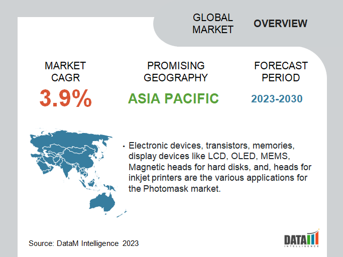
The global photomask market, essential to photolithography in semiconductors and displays, reached USD 5.1 billion in 2024, and is expected to hit USD 7.0 billion by 2033, growing at a CAGR of 3.5% from 2025 to 2033. According to Grand View Research, market size exceeded USD 5.11 billion in 2023, with a faster CAGR of 4.7% predicted through 2030.

Photomask-Market-Overview
Request a sample copy of research report: https://www.datamintelligence.com/download-sample/photomask-market
🔍 Key Market Drivers
1. Chip Miniaturization & Advanced Lithography
Advanced semiconductor processes—5 nm, 3 nm, and emerging 2 nm nodes—rely on high-precision photomasks. EUV lithography especially demands intricate reticles . As chips shrink, the need for detailed patterning intensifies, bolstering photomask demand.
2. Rising Demand from AI, 5G, IoT & EVs
Semiconductor use in AI processors, 5G infrastructure, IoT devices, EV sensors, ADAS, MEMS, and displays is accelerating. These applications produce a surge in photomask requirements.
3. Displays & Foldable Screen Innovation
Displays, including OLED, LCD, and emerging foldable technologies, accounted for 33.1% of photomask applications in 2023 . Complex display patterns demand high-resolution reticles, further pushing the market.
4. Regional Production Scale-Up
Asia-Pacific encompasses 36.6% of global photomask revenue in 2024 and is projected to grow to USD 2.8 million by 2030, thanks to strong semiconductor manufacturing expansion.
North America accounted for 28% of global market revenues in 2024, rising from USD 1.5 M to an expected USD 2.1 M by 2030 (CAGR 5.6%), driven by U.S. *** in AI chips, consumer electronics, and automotive semiconductors.
🚀 Regional Trends: US, Canada & Japan
🇺🇸 United States & Canada
North America maintains a high-precision chip manufacturing ecosystem. *** in EUV, high-NA reticles, data centers, and automotive electronics fuels strong photomask demand.
🇯🇵 Japan
Japan remains a key player in semiconductor infrastructure and mask technology, contributing significantly to APAC’s dominance. However, Japanese commercial equipment firms have evolved their strategy around EUV, with high-NA initiatives in progress.
📑 Product & Application Breakdown
Product Type:
-
Reticles – held 62.1% market share in 2023. They serve as scaled-up masks for EUV lithography.
-
Master Masks are also growing, especially for MEMS and display applications.
Applications:
-
Displays – largest application at 33.1%.
-
Discrete Components, Optical Devices, MEMS – rising demand in automotive sensors and industry 4.0 applications.
💡 Industry Trends & Innovations
High‑NA EUV & Larger Mask Formats
Efforts toward larger format and high‑NA EUV masks, like Intel and ASML’s move to 6"×12" masks, boost performance and reduce stitching errors.
Captive vs Merchant Mask Shops
Captive mask shops (Intel, Samsung, TSMC) handle advanced nodes; merchant shops serve smaller nodes. Shortages at mature nodes like 16/14 nm highlight supply chain vulnerabilities.
Collaborative R&D
Tekscend (formerly Toppan Photomasks) joined IBM in 2024 to develop 2 nm logic node masks, focusing on High‑NA EUV advancements.
📊 Market Forecast & Competitive Insights
|
Metric |
Value |
|
2024 Market Size |
USD 5.1 B (IMARC) / USD 5.11 B (GVR) |
|
2024–2030 CAGR |
4.7% (GVR); 3.5% (IMARC 2025–33) |
|
2025 Size Estimate |
USD 6.08 B (Mordor) |
|
2030 Forecast |
USD 7.44 B (GVR); USD 7.59 B (Mordor) |
|
North America CAGR |
5.6% to 2030 |
|
Asia-Pacific CAGR to 2030 |
5.7% |
Major players include Tekscend, Dai Nippon Printing, Photronics, HOYA, Applied Materials, KLA, LG Innotek, Nippon Filcon, SK-Electronics.
📌 Challenges & Opportunities
High Cost & Precision Requirements
EUV-ready masks demand *** in electron-beam writing and quality control. Costs limit smaller semiconductor makers.
Geopolitical & Supply Chain Risks
Trade tensions highlight need for localized production. US CHIPS Act and Japanese semiconductor policy support domestic capacity.
Growth in Niche Segments
MEMS, automotive electronics, sensors, and defense sectors offer specialized mask growth, especially in North America and Europe.
Request a Quotation: https://www.datamintelligence.com/buy-now-page?report=photomask-market
🏁 Outlook
The photomask market stands at a pivotal moment—valued at USD 5.1 B in 2024, with multiple ***ysts forecasting expansion to USD 7–7.6 B by 2030–33, driven by AI, 5G, EV, and display waves, underpinned by miniaturization trends.
Advanced lithography (High‑NA EUV), strategic alliances, and regional semiconductor ***s (notably in the US and Japan) are steering market resilience. Ongoing evolution toward high-performance chips and more complex masks will continue fueling demand—even as costs and supply chain constraints challenge the industry.

