

Laser Debonding Equipment Market Size, Share & Research Report (2025–2033) | UnivDatos
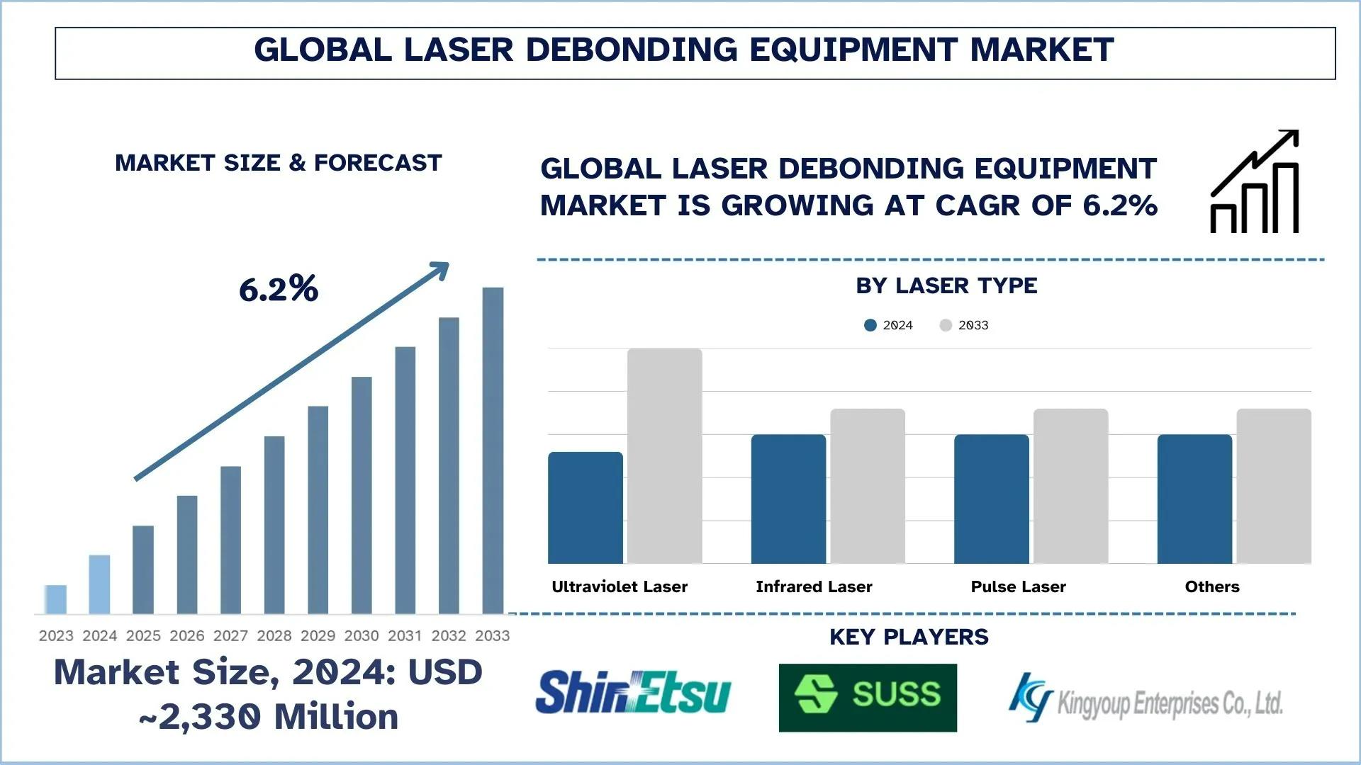
According to the UnivDatos, the rising demand for laser debonding among the end-user industries would fuel the demand for Laser Debonding Equipment to grow. As per their “Laser Debonding Equipment Market” report, the global market was valued at USD 2,330 million in 2024, growing at a CAGR of about 6.2% during the forecast period from 2025 - 2033 to reach USD million by 2033.
The laser debonding equipment market is changing rapidly due to technological advances and increasing demand for modern electronics manufacturing. Laser debonding is now considered one of the critical enablers for advanced semiconductor packaging because the next generation of high-performance, compact, and thermally efficient devices poses the most severe challenges that need to be overcome. 3D ICs, SiP, and FOWLP integrate into the next generation of devices, which highly require the use of non-contact separation techniques that are precise and damage-free, like laser technology solutions. Moreover, technology needs to be integrated into a high-throughput solution because of its non-contact processing and high accuracy, making it ideal for making delicate, high-density wafer handling work well with automation. Finally, the transformation is being further propelled by smart manufacturing trends and is even being extended to other sectors of applications.
Access sample report (including graphs, charts, and figures): https://univdatos.com/reports/laser-debonding-equipment-market?popup=report-enquiry
Advancements in Semiconductor Packaging:
Over the last few years, semiconductor packaging has witnessed significant changes, owing to the demand for next-generation electronic devices with high power levels, compact dimensions, and efficient ***gns. Yet, traditional packaging conventions are being replaced by radical approaches such as 3D Integrated Circuits (3D ICs), System-in-Package (SiP), and Fan-Out Wafer-Level Packaging (FOWLP). These advanced technologies offer high transistor density, better electrical performance, and good thermal management for next-generation devices such as smartphones, data centers, AI processors, and IoT components.
Laser debonding systems have been instrumental in the advanced packaging processes. Bonding substrates transiently is common during wafer handling and processing. Laser debonding represents the most precise method of debonding these structures without contacting and harming fragile structures. This becomes especially important in the context of thin-wafer applications, where any mechanical stress via conventional debonding methods could end up breaking the wafer and consequently lead to a loss of yield.
Needless to say, as chip manufacturers shrink die dimensions and make their performance more demanding, the pressure on these debonding methods becomes stronger. These laser-based methods provide reliable, efficient, and damage-free debonding with the required precision and speed for successful integration into automated manufacturing systems. Laser debonding equipment is thus an integral enabling technology for the domain of semiconductor packaging technology going forward.
Latest Trends in the Laser Debonding Equipment Market
Technological Innovations in Laser Systems:
Ongoing innovations in laser technology are indeed molding the market for laser debonding equipment. Such techniques as ultrafast pulsed lasers, laser-induced breakdown spectroscopy (LIBS), and advanced beam shaping now heighten the precision, speed, and versatility of laser systems. These constitute a cleaner, more controlled material separation, even taking into account the reduced incidence of thermal damage to sensitive substrates during the debonding processes. Moreover, innovations in automation and real-time feedback systems, further enhanced with AI, are engaging in better process control and yield improvement. Such technological improvement is necessary to meet the stringent specifications of next-generation electronic devices, where very thin wafers, with very high component density, leave little margin for error, compelling manufacturers to seek more advanced laser systems not only for quality improvement but also for reduced downtime and maintenance. Thus, a much tougher, faster, and more efficient production environment customized according to modern semiconductors and electronics use is realized.
Expansion into Diverse Industries:
Traditionally known for application in semiconductor and consumer electronics manufacturing, laser debonding equipment is being utilized in a wider spectrum of industries. For example, this technology in the medical devices sector allows for fine, delaminating materials employed in implants, diagnostic equipment, and micro-surgical tools while at the same time not subjecting them to any mechanical stress or contamination. Laser debonding will soon also feature in the automotive and aerospace industries since they want to target advanced manufacturing processes of lightweight materials and multi-layer components. The growth of flexible electronics and wearable technologies is indeed contributing to an increasing demand for precision debonding solutions applicable to nontraditional substrates, while the other applications stem from the increasing miniaturization, the need for reliability, and cleanroom-compatible manufacturing across borders. Consequently, equipment manufacturers continue to make specialized systems for various use cases, broadening the market reach of laser debonding and securing its role in the future of high-tech manufacturing.
Regional Market Growth
The North America laser debonding equipment market is benefiting from the emergence of the industries in semiconductors, electronics, and advanced manufacturing. Most notably, the US comprises a lot of key stakeholders in semiconductor manufacturing and R&D as well, thereby necessitating precision and efficiency in laser-based debonding technology, particularly due to the encouraging scenario of chipmakers toward smaller node technologies, advanced packaging, and thinner wafers. Laser debonding provides excellent advantages, such as high accuracy in non-contact processing and very little damage to the substrate.
North America is an early adopter of newer technologies, ranging from automation to Industry 4.0 and AI-integrated production systems. The overall process efficiency and yield achieved across manufacturing lines have further improved with laser debonding equipment integrated with automated handling tools and AI-driven quality inspection systems. In addition, the growth of the application of laser debonding in medical device manufacturing and aerospace electronics is also expected to drive the growth of the regional market.
***s into homegrown semiconductor manufacturing- most recently catalyzed by the U.S. CHIPS and Science Act-promises to drive further demand for cutting-edge debonding solutions. Equally compelling is the kind of collaboration that is spurring research and industry partnerships to push the frontiers of innovation in laser processing technology. Thus, the market for laser debonding equipment considers North America as a key geographical location among all important ones in terms of growth figures.
Click here to view the Report Description & TOC https://univdatos.com/reports/laser-debonding-equipment-market
Shaping the Future of Manufacturing: The Growing Role of Laser Debonding Equipment in Precision Industries:
While laser debonding equipment is poised to drive the shift towards miniaturization, automation, and high-reliability electronics in global industry, its growing importance is felt in semiconductors, medical devices, aerospace, and flexible electronics through the demand for precision and cleanroom-compatible processes. With important government initiatives, including the CHIPS Act, fostering growth in North America due to the technological leadership in the region, there will be a continued focus on developments in laser technology, AI integration, and application-oriented system ***gn, which will ensure that laser debonding is critical to next-generation manufacturing. On this dynamic stage, laser debonding appears not just as an instrument but as a strategic enabler for innovations and scalability.
Related Report:-
Laser-Induced Breakdown Spectroscopy Market: Current ***ysis and Forecast (2023-2030)
Welding Torch and Tip Changing Robotic Station Market: Current ***ysis and Forecast (2024-2032)
Tunable Laser Market: Current ***ysis and Forecast (2023-2030)
Industrial Automation Market: Current ***ysis and Forecast (2024-2032)
MENA Manufacturing 3D Printing Market: Current Scenario and Forecast (2019-2025)
Contact Us:
UnivDatos
Contact Number - +1 978 733 0253
Email - contact@univdatos.com
Website - www.univdatos.com
Linkedin- https://www.linkedin.com/company/univ-datos-market-insight/mycompany/

